
Home >> My Performance >> My Topic Test Performance >> My Question Performance
My Question Performance Summary in Full Tests !
Questions Available: 29
Questions Attempted: 10
Number of Attempts: 15
Correct Attempts: 8
Total Time Spent: 00:30
Avg Time Per Question: 00:02
My Question Performance Summary in Full Tests
Given below are two statements:
Statement I:Photovoltaic devices can convert optical radiation into electricity.
Statement II:Zener diode is designed to operate under reverse bias in breakdown region. In the light of the above statements, choose the most appropriate answer from the options given below.
(1). Both Statement I and Statement II are incorrect
(2). Statement I is correct but Statement II is incorrect
(3). Statement I is incorrect but Statement II is correct
(4). Both Statement I and Statement II are correct
Number of Attempts: 2
Correct Attempts: 1
Time Taken: 00:04
Average Time: 00:02
A full wave rectifier circuit consists of two p-n junction diodes, a centre-tapped transformer, capacitor and a load resistance. Which of these components remove the ac ripple from the rectified output?
(1). p-n junction diodes
(2). Capacitor
(3). Load resistance
(4). A centre-tapped transformer
(1). p-n junction diodes
(2). Capacitor
(3). Load resistance
(4). A centre-tapped transformer
Number of Attempts: 2
Correct Attempts: 1
Time Taken: 00:04
Average Time: 00:02
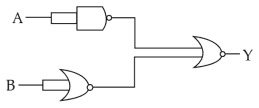
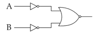
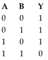
The output (Y) of the given logic implementation is similar to the output of an/a _______ gate.
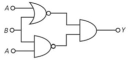
(1). NOR
(2). AND
(3). NAND
(4). OR
(1). NOR
(2). AND
(3). NAND
(4). OR
Number of Attempts: 2
Correct Attempts: 1
Time Taken: 00:04
Average Time: 00:02
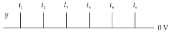
A full wave rectifier circuit with diodes (\(\text{D}_1\)) and (\(\text{D}_2\)) is shown in the figure. If input supply voltage \(\text{V}_\text{in}\,=\,220\,sin\left(100\pi \text{t}\right)\) volt, then at t= 15 msec
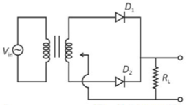
(1). (\(\text{D}_1\)) and (\(\text{D}_2\)) both are reverse biased
(2). (\(\text{D}_1\)) is forward biased, (\(\text{D}_2\)) is reverse biased
(3). (\(\text{D}_1\)) is reverse biased, (\(\text{D}_2\)) is forward biased
(4). (\(\text{D}_1\)) and (\(\text{D}_2\)) both are forward biased
(1). (\(\text{D}_1\)) and (\(\text{D}_2\)) both are reverse biased
(2). (\(\text{D}_1\)) is forward biased, (\(\text{D}_2\)) is reverse biased
(3). (\(\text{D}_1\)) is reverse biased, (\(\text{D}_2\)) is forward biased
(4). (\(\text{D}_1\)) and (\(\text{D}_2\)) both are forward biased
Number of Attempts: 2
Correct Attempts: 1
Time Taken: 00:04
Average Time: 00:02
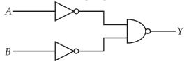
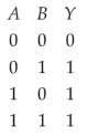
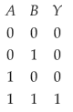
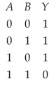
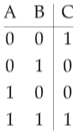
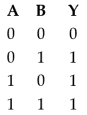
A logic circuit provides the output Y as per the following truth table :
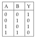
The expression for the output Y is
(1). \(A⋅B+\bar{A}\)
(2). \(\displaystyle A⋅\bar{B}+\bar{A}\)
(3). \(\displaystyle \bar{B} \)
(4). B
The expression for the output Y is
(1). \(A⋅B+\bar{A}\)
(2). \(\displaystyle A⋅\bar{B}+\bar{A}\)
(3). \(\displaystyle \bar{B} \)
(4). B
Number of Attempts: 2
Correct Attempts: 1
Time Taken: 00:04
Average Time: 00:02
Consider the following statements A and B and identify the correct answer:
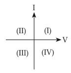
A. For a solar-cell, the I-V characteristics lies in the IV quadrant of the given graph.
B. In a reverse biased pn junction diode, the current measured (in µA), is due to majority charge carriers.
(1). A is correct but B is incorrect
(2). A is incorrect but B is correct
(3). Both A and B are correct
(4). Both A and B are incorrect
Number of Attempts: 2
Correct Attempts: 1
Time Taken: 00:04
Average Time: 00:02
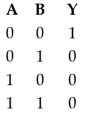
The output (Y) of the given logic gate is similar to the output of an/a
(1). NAND gate
(2). NOR gate
(3). OR gate
(4). AND gate
(1). NAND gate
(2). NOR gate
(3). OR gate
(4). AND gate
Number of Attempts: 2
Correct Attempts: 1
Time Taken: 00:04
Average Time: 00:02
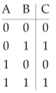
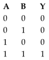
For the following logic circuit, the truth table is
(1).
(2).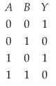
(3).
(4).
(1).
(2).
(3).
(4).
Number of Attempts: 2
Correct Attempts: 1
Time Taken: 00:04
Average Time: 00:02
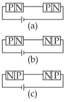
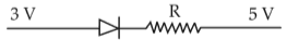
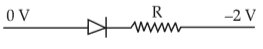
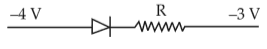
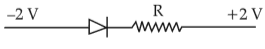
In the given circuits (a), (b), and (c), the potential drop across the two p − n junctions are equal in
(1). Circuit (a) only
(2). Circuit (b) only
(3). Circuit (c) only
(4). Both circuits (a) and (c)
Number of Attempts: 2
Correct Attempts: 1
Time Taken: 00:04
Average Time: 00:02
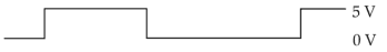
In half wave rectification, if the input frequency is 60 Hz, then the output frequency would be
(1). Zero
(2). 30 Hz
(3). 60 Hz
(4). 120 Hz
(1). Zero
(2). 30 Hz
(3). 60 Hz
(4). 120 Hz
Number of Attempts: 2
Correct Attempts: 1
Time Taken: 00:04
Average Time: 00:02
The truth table for the given logic circuit is
(1).

(2).
(3).
(4).
Number of Attempts: 2
Correct Attempts: 1
Time Taken: 00:04
Average Time: 00:02
The electron concentration in an n-type semiconductor is the same ashole concentration in a p-type semiconductor. An external field(electric) is applied across each of them. Compare the currents in them.
(1). Current in n-type = current in p-type
(2). Current in p-type > current in n-type
(3). Current in n-type > current in p-type
(4). No current will flow in p-type, current will only flow in n-type
(1). Current in n-type = current in p-type
(2). Current in p-type > current in n-type
(3). Current in n-type > current in p-type
(4). No current will flow in p-type, current will only flow in n-type
Number of Attempts: 2
Correct Attempts: 1
Time Taken: 00:04
Average Time: 00:02
Consider the following statements (A) and (B) and identify the correct answer.
(A). A zener diode is connected in reverse bias, when used as a voltage regulator.
(B). The potential barrier of p-n junction lies between 0.1 V to 0.3 V.
(1). (A) and (B) both are correct.
(2). (A) and (B) both are incorrect
(3). (A) is correct and (B) is incorrect.
(4). (A) is incorrect but (B) is correct.
Number of Attempts: 2
Correct Attempts: 1
Time Taken: 00:04
Average Time: 00:02
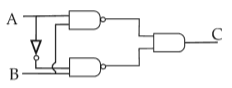
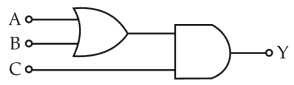
For the given circuit, the input digital signals are applied at theterminals A, B and C. What would be the output at the terminal y ?
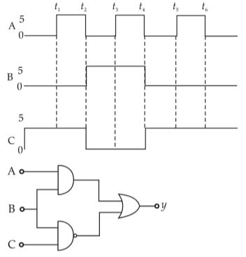
(1).
(2).
(3).
(4).
(1).
(2).
(3).
(4).
Number of Attempts: 2
Correct Attempts: 1
Time Taken: 00:04
Average Time: 00:02
The increase in the width of the depletion region in a p-n junction diodeis due to:
(1). reverse bias only
(2). both forward bias and reverse bias
(3). increase in forward current
(4). forward bias only
(1). reverse bias only
(2). both forward bias and reverse bias
(3). increase in forward current
(4). forward bias only
Number of Attempts: 2
Correct Attempts: 1
Time Taken: 00:04
Average Time: 00:02
For transistor action, which of the following statements is correct?
(1). Base, emitter and collector regions should have same size.
(2). Both emitter junction as well as the collector junction are forward biased
(3). The base region must be very thin and lightly doped
(4). Base, emitter and collector regions should have same doping concentrations.
(1). Base, emitter and collector regions should have same size.
(2). Both emitter junction as well as the collector junction are forward biased
(3). The base region must be very thin and lightly doped
(4). Base, emitter and collector regions should have same doping concentrations.
Number of Attempts: 2
Correct Attempts: 1
Time Taken: 00:04
Average Time: 00:02
For the logic circuit shown, the truth table is:
(1).
(2).
(3).
(4).
(1).
(2).
(3).
(4).
Number of Attempts: 2
Correct Attempts: 1
Time Taken: 00:04
Average Time: 00:02
The energy required to break one bond in DNA is \(10^{-20}\, \text{J}\). This value in eV is nearly
(1). 0.6
(2). 0.06
(3). 0.006
(4). 6
(1). 0.6
(2). 0.06
(3). 0.006
(4). 6
Number of Attempts: 2
Correct Attempts: 1
Time Taken: 00:04
Average Time: 00:02
For a p -type semiconductor, which of the following statements is true?
(1). Electrons are the majority carriers and pentavalent atoms are the dopants.
(2). Electrons are the majority carriers and trivalent atoms are the dopants.
(3). Holes are the majority carriers and trivalent atoms are the dopants.
(4). Holes are the majority carriers and pentavalent atoms are the dopants.
Number of Attempts: 2
Correct Attempts: 1
Time Taken: 00:04
Average Time: 00:02
The correct Boolean operation represented by the circuit diagramdrawn is
(1). NOR
(2). AND
(3). OR
(4). NAND
Number of Attempts: 2
Correct Attempts: 1
Time Taken: 00:04
Average Time: 00:02
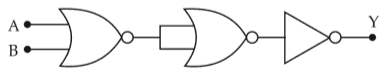
In the combination of the following gates the output Y can be written in terms of inputs A and B as
(1).
(2).
(3).
(4).
(1).
(2).
(3).
(4).
Number of Attempts: 2
Correct Attempts: 1
Time Taken: 00:04
Average Time: 00:02
In the circuit shown in the figure,
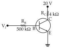
the input voltage \(V_i\) is 20 V , \(V_{BE}\) = 0 and \(V_{CE}\) = 0. The values of \(I_B\), \(I_C\)and β are given by
(1). \(I_B = 40µA, I_C = 10mA, β = 250\)
(2). \(I_B = 25µA, I_C = 5mA, β = 200\)
(3). \(I_B = 20µA, I_C = 5mA, β = 250\)
(4). \(I_B = 40µA, I_C = 5mA, β = 125\)
the input voltage \(V_i\) is 20 V , \(V_{BE}\) = 0 and \(V_{CE}\) = 0. The values of \(I_B\), \(I_C\)and β are given by
(1). \(I_B = 40µA, I_C = 10mA, β = 250\)
(2). \(I_B = 25µA, I_C = 5mA, β = 200\)
(3). \(I_B = 20µA, I_C = 5mA, β = 250\)
(4). \(I_B = 40µA, I_C = 5mA, β = 125\)
Number of Attempts: 2
Correct Attempts: 1
Time Taken: 00:04
Average Time: 00:02
In a p − n junction diode, change in temperature due to heating
(1). affects only reverse resistance
(2). affects only forward resistance
(3). does not affect resistance of p − n junction
(4). affects the overall V - I characteristics of p − n junction
(1). affects only reverse resistance
(2). affects only forward resistance
(3). does not affect resistance of p − n junction
(4). affects the overall V - I characteristics of p − n junction
Number of Attempts: 2
Correct Attempts: 1
Time Taken: 00:04
Average Time: 00:02
In a common emitter transistor amplifier the audio signal voltage across the collector is 3 V. The resistance of collector is 3 KΩ. If current gain is 100 and the base resistance is 2 KΩ, the voltage and power gain of the amplifier is
(1). 15 and 200
(2). 150 and 15000
(3). 20 and 2000
(4). 200 and 1000
(1). 15 and 200
(2). 150 and 15000
(3). 20 and 2000
(4). 200 and 1000
Number of Attempts: 2
Correct Attempts: 1
Time Taken: 00:04
Average Time: 00:02
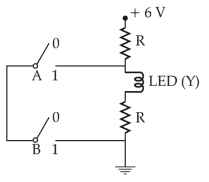
The given electrical network is equivalent to
(1). OR gate
(2). NOR gate
(3). NOT gate
(4). AND gate
(1). OR gate
(2). NOR gate
(3). NOT gate
(4). AND gate
Number of Attempts: 2
Correct Attempts: 1
Time Taken: 00:04
Average Time: 00:02
Which one of the following represents forward bias diode?
(1).
(2).
(3).
(4).
(1).
(2).
(3).
(4).
Number of Attempts: 2
Correct Attempts: 1
Time Taken: 00:04
Average Time: 00:02
To get output 1 for the following circuit, the correct choice for the inputis
(1). A = 1,B = 1, C = 0
(2). A = 1, B = 0, C= 1
(3). A = 0, B = 1,C = 0
(4). A = 1 , B = 0, C = 0
(1). A = 1,B = 1, C = 0
(2). A = 1, B = 0, C= 1
(3). A = 0, B = 1,C = 0
(4). A = 1 , B = 0, C = 0
Number of Attempts: 2
Correct Attempts: 1
Time Taken: 00:04
Average Time: 00:02
A npn transistor is connected in common emitter configuration in a given amplifier. A load resistance of \(800\, \Omega\) is connected in the collector circuit and the voltage drop across it is \(0.8\, \text{V}\). If the current amplification factor is \(0.96\) and the input resistance of the circuit is \(192\, \Omega\), the voltage gain and the power gain of the amplifier will respectively be
(1). 4, 4
(2). 4, 3.69
(3). 4, 3.84
(4). 3.69, 3.84
(1). 4, 4
(2). 4, 3.69
(3). 4, 3.84
(4). 3.69, 3.84
Number of Attempts: 2
Correct Attempts: 1
Time Taken: 00:04
Average Time: 00:02
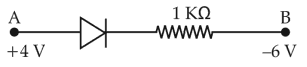
Consider the junction diode as ideal. The value of current flowing through AB is
(1). \(10^{−1}\,A\)
(2). \(10^{−3}\,A\)
(3). \(0\,A\)
(4). \(10^{−2}\,A\)
(1). \(10^{−1}\,A\)
(2). \(10^{−3}\,A\)
(3). \(0\,A\)
(4). \(10^{−2}\,A\)
Number of Attempts: 2
Correct Attempts: 1
Time Taken: 00:04
Average Time: 00:02