Home >> Topics >> Semiconductor electronics: Materials, devices and simple circuits
Unattempted Questions
Questions Available: 29
Year: 2023
Topic: Semiconductor electronics: Materials, devices and simple circuits
1.
Given below are two statements:
Statement I:Photovoltaic devices can convert optical radiation into electricity.
Statement II:Zener diode is designed to operate under reverse bias in breakdown region. In the light of the above statements, choose the most appropriate answer from the options given below.
Statement I:Photovoltaic devices can convert optical radiation into electricity.
Statement II:Zener diode is designed to operate under reverse bias in breakdown region. In the light of the above statements, choose the most appropriate answer from the options given below.
Solution
Year: 2023
Topic: Semiconductor electronics: Materials, devices and simple circuits
2.
A full wave rectifier circuit consists of two p-n junction diodes, a centre-tapped transformer, capacitor and a load resistance. Which of these components remove the ac ripple from the rectified output?
Solution
Solution
Year: 2025
Topic: Semiconductor electronics: Materials, devices and simple circuits
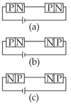
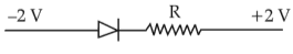
4.
A full wave rectifier circuit with diodes (\(\text{D}_1\)) and (\(\text{D}_2\)) is shown in the figure. If input supply voltage \(\text{V}_\text{in}\,=\,220\,sin\left(100\pi \text{t}\right)\) volt, then at t= 15 msec
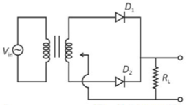
Solution
Solution
Year: 2024
Topic: Semiconductor electronics: Materials, devices and simple circuits
6.
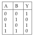
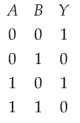
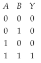
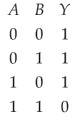
Consider the following statements A and B and identify the correct answer:
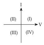
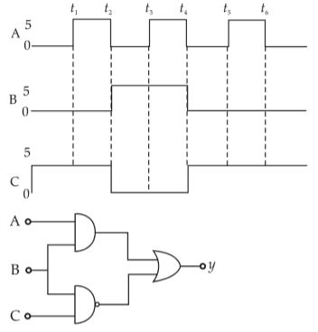
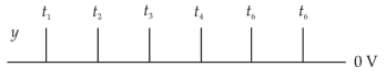
A. For a solar-cell, the I-V characteristics lies in the IV quadrant of the given graph.
B. In a reverse biased pn junction diode, the current measured (in µA), is due to majority charge carriers.
A. For a solar-cell, the I-V characteristics lies in the IV quadrant of the given graph.
B. In a reverse biased pn junction diode, the current measured (in µA), is due to majority charge carriers.
Solution
Solution
Solution
Solution
Solution

Solution
Year: 2021
Topic: Semiconductor electronics: Materials, devices and simple circuits
12.
The electron concentration in an n-type semiconductor is the same ashole concentration in a p-type semiconductor. An external field(electric) is applied across each of them. Compare the currents in them.
Solution
Year: 2021
Topic: Semiconductor electronics: Materials, devices and simple circuits
13.
Consider the following statements (A) and (B) and identify the correct answer.
(A). A zener diode is connected in reverse bias, when used as a voltage regulator.
(B). The potential barrier of p-n junction lies between 0.1 V to 0.3 V.
(A). A zener diode is connected in reverse bias, when used as a voltage regulator.
(B). The potential barrier of p-n junction lies between 0.1 V to 0.3 V.
Solution

Solution
Solution
Solution
Solution
Solution
Solution
Solution


Solution
Solution
Solution
Year: 2017
Topic: Semiconductor electronics: Materials, devices and simple circuits
24.
In a common emitter transistor amplifier the audio signal voltage across the collector is 3 V. The resistance of collector is 3 KΩ. If current gain is 100 and the base resistance is 2 KΩ, the voltage and power gain of the amplifier is
Solution
Solution
Solution
Solution
Year: 2016
Topic: Semiconductor electronics: Materials, devices and simple circuits
28.
A npn transistor is connected in common emitter configuration in a given amplifier. A load resistance of \(800\, \Omega\) is connected in the collector circuit and the voltage drop across it is \(0.8\, \text{V}\). If the current amplification factor is \(0.96\) and the input resistance of the circuit is \(192\, \Omega\), the voltage gain and the power gain of the amplifier will respectively be